
This application note describes the solderability tests performed on STMicroelectronics lead-free devices, and how to form a reliable solder joint with the base material of the circuit board, using lead-free (Sn-Ag-Cu) or leaded (Sn-Pb) solder.
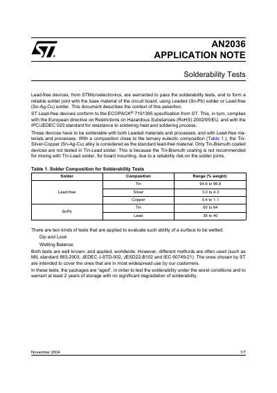
This document details the solderability tests applied to STMicroelectronics lead-free devices to ensure they form reliable solder joints with both leaded (Sn-Pb) and lead-free (Sn-Ag-Cu) solders. The devices conform to the ECOPACK specification and comply with RoHS directives.
Two primary tests are described: the "Dip and Look" test, which inspects surface coverage after dipping in molten solder, and the "Wetting Balance" test, which measures the force exerted during immersion to determine wetting time. Specific test conditions, such as aging procedures and solder temperatures, are provided for both surface mount and insertion packages.
| Solder Composition Range (Lead-free) | Tin 94.6 to 96.6, Silver 3.0 to 4.3, Copper 0.4 to 1.1 |
|---|---|
| Solder Composition Range (SnPb) | Tin 60 to 64, Lead 36 to 40 |
| Lead-free Solder Melting Temperature | 245°C |
| Leaded Solder Melting Temperature | 220°C |
| Wetting Force Criterion | 0.1mN/mm within 5 seconds |
| Zero Cross Time Criterion | Less than 3 seconds |
The test is considered passed if 95% of the surface is covered with fresh solder.
No, they are not tested because mixing them with Tin-Lead solder poses a reliability risk.