
STMicroelectronics AN394 MICROWIRE EEPROM Common I/O Operation Application Note

This application note provides information regarding common I/O operation of the MICROWIRE® EEPROM family of products. This information can help designers interface MICROWIRE® EEPROM products with different microcontrollers.
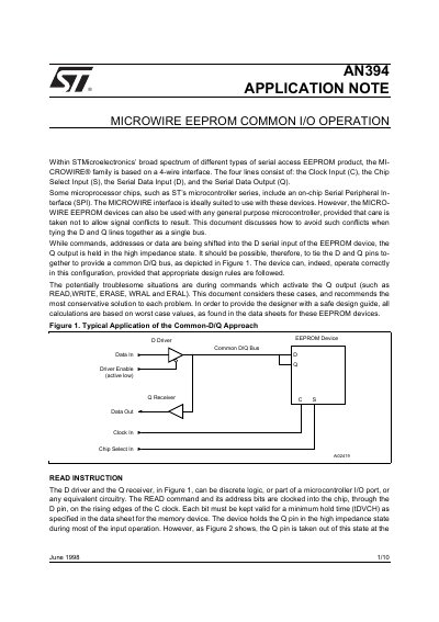

STMicroelectronics AN394 MICROWIRE EEPROM Common I/O Operation Application Note - cover page
Brand
STMicroelectronics
Category
Memory
Document type
Application Note
Language
English
Pages
10
File format
PDF
File size
72 KB
Published
06 August, 2012
Updated
30 September, 2023
MD5 checksum
F41FD4A611E49700E800C6557292B65A

About this manual

The document addresses the design challenges of connecting the Serial Data Input (D) and Serial Data Output (Q) lines of STMicroelectronics MICROWIRE EEPROMs to a single common bus. It identifies potential signal conflicts during read operations where the output buffer activates while input data is still being shifted in, which can cause short-circuits or undefined logic levels.

What's inside

  • Common D/Q Bus Operation
  • READ Instruction Timing
  • Bus Conflict Resolution
  • Current Limiting Resistor Placement
  • Interface with CMOS Circuits
  • Pull-up Resistor Considerations

Frequently asked questions

What is the recommended location for the current limiting resistor in a common D/Q bus?

The best location is between the Q output and the D/Q bus to allow the D driver to override the Q driver during overlap.

What is the minimum delay required before sampling the data line after a clock rising edge?

The delay should be at least 3xRC to ensure stable logic levels on the bus.

How does the resistor value affect the clock frequency during a READ operation?

The maximum clock frequency is directly related to the RC time constant, potentially requiring reduction by an amount proportional to it.

Download PDF (72 KB)

More STMicroelectronics Manuals


View all STMicroelectronics manuals →