
This application note introduces the STLC3055N single supply SLIC features and applications. STLC3055N is a slic device specially designed for WLL ( Wireless Local Loop) and ISDN Terminal Adapters.
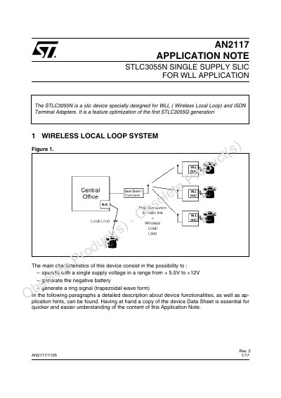
This document is an application note for the STLC3055N, a Single Line Interface Circuit (SLIC) device designed for Wireless Local Loop (WLL) and ISDN Terminal Adapters. It details the device's ability to operate with a single supply voltage and generate negative battery voltages and ring signals.
The text provides typical application schematics, explains the DC-DC converter operation, and discusses input current limitation techniques. It includes specific data on thermal resistance, voltage generation tables for active and ring modes, and performance characteristics for driving various ringer loads (1REN to 5REN) at different supply voltages.
| Supply Voltage Range | +5.5V to +12V |
|---|---|
| Thermal Resistance (Full plastic TQFP on single layer board) | 70 °C/W |
| Thermal Resistance (Full plastic TQFP on four layer board) | 45 °C/W |
| Maximum Duty Cycle | about 95% |
| Output Current Limitation (Peak) | about 80mA |
| Ringing Frequency (Typical) | 20/25Hz |
It is specially designed for WLL (Wireless Local Loop) and ISDN Terminal Adapters.
Yes, it can generate a ring signal with a trapezoidal waveform.
It is defined by the voltage divider RF1, RF2 and can be set choosing a proper value of RF1.
The settling time is about 150ms and is a function of the CAC splitter capacitor.