
This EE-Note is intended to help the user select and configure a suitable Synchronous Dynamic Random Access Memory (SDRAM) device to interface with Analog Devices Inc. (ADI) processors and DSPs. This document discusses the different factors involved in choosing the appropriate memory component depending on the Processor or DSP used. Additionally, some programming examples on how to configure the SDRAM are provided.
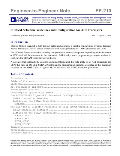
This Engineer-to-Engineer Note (EE-210) assists users in selecting and configuring Synchronous Dynamic Random Access Memory (SDRAM) devices to interface with Analog Devices Inc. (ADI) processors and DSPs. It discusses the factors involved in choosing appropriate memory components based on the specific processor or DSP used. Additionally, the document provides programming examples on how to configure the SDRAM controller for specific ADI processors.
The note focuses on the ADSP-TS201S TigerSHARC and the ADSP-BF533 Blackfin processors, detailing their on-chip SDRAM controller features. It covers specifications such as supported operating voltage, maximum frequency, memory size, CAS latency, and refresh rates. The document includes compatibility tables and register setting instructions for configuring the SDRAM controller.
| Supported operating Voltage | 3.3 and 2.5 V |
|---|---|
| Maximum supported operating Frequency | 125 MHz |
| Maximum supported memory | 256 Mbytes per external SDRAM bank |
| Number of internal SDRAM banks | 2 or 4 banks |
| Column Address Strobe (CAS) latency | 1 to 3 system clock cycles |
| Refresh rate | 32 to 64 ms |
The ADSP-21065L and ADSP-21161N SHARC DSPs, the ADSP-TS101S, ADSP-TS201S, ADSP-TS202S and ADSP-TS203S TigerSHARC processors, and the ADSP-BF531, ADSP-BF532, ADSP-BF533 and ADSP-BF535 Blackfin processors.
The maximum supported memory is 256 Mbytes (64 M x 32 bits or 32 M x 64 bits) per external SDRAM bank.
The Column Address Strobe (CAS) latency is programmable to a value of 1 to 3 system clock cycles (SCLK).