
This document is the ADL5304 evaluation board user guide, which introduces the functions and features of the evaluation board, including circuit principles, performance parameters and application scenarios.
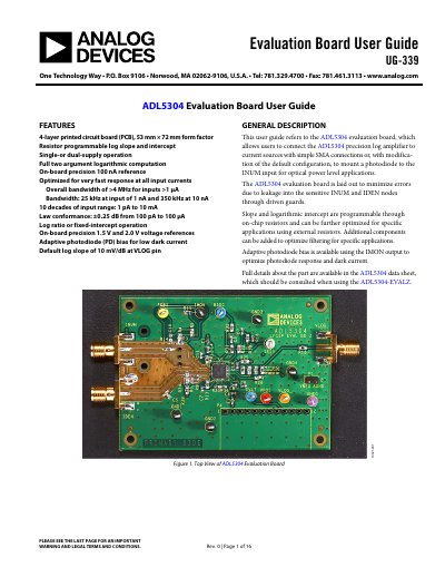
The ADL5304 evaluation board allows users to connect the precision log amplifier to current sources or photodiodes. It features a 4-layer PCB with a 53 mm × 72 mm form factor and supports single or dual-supply operation. The board includes programmable log slope and intercept via on-chip resistors and an on-board precision 100 nA reference.
| PCB Form Factor | 53 mm × 72 mm |
|---|---|
| Input Range (Single Supply) | 1 pA to 3 mA |
| Input Range (Dual Supply) | 1 pA to 10 mA |
| Bandwidth (>1 μA) | >4 MHz |
| Bandwidth (1 nA) | 25 kHz |
| Bandwidth (10 nA) | 350 kHz |
| Law Conformance | ±0.25 dB |
| Default Log Slope | 10 mV/dB |
In single-supply configuration, the VNEG bus is connected to ground using Jumper P1.
Remove Jumper P1 and connect the VNEG supply to a −2 V to −5 V source.
The log slope is programmed using internal resistors accessed by placing 0 Ω resistors in positions R24 to R28.
The IMON output provides an adaptive photodiode bias scheme by multiplying the input current by 1.1.