
Analog Devices ADP199 High-Side Load Switch Evaluation Board User Guide UG-336

This document introduces the features and characteristics of the ADP199 high-side load switch, including its ultrasmall size, low RDSON, low input voltage range, 500mA continuous operating current, and -40℃ to +85℃ operating temperature range.
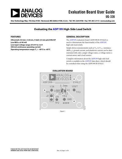

Analog Devices ADP199 High-Side Load Switch Evaluation Board User Guide UG-336 - cover page
Brand
Analog Devices
Category
Other Electronics
Document type
User Manual
Language
English
Pages
8
File format
PDF
File size
266 KB
Published
02 August, 2012
Updated
30 September, 2023
MD5 checksum
9B1EA31390ADD93801E111C81D7809A1

About this manual

The document provides a user guide for the ADP199 High-Side Load Switch Evaluation Board (ADP199CB-EVAL). The board is designed to demonstrate the functionality of the ADP199 chip, allowing users to perform simple device measurements such as on-resistance (RDS ON), ground current, and shutdown current using a single voltage source, meters, and a load resistor.

What's inside

  • Features
  • General Description
  • Evaluation Board Schematic and Hardware
  • VIN to V OUT Resistance Measurements
  • Ground Current Measurements
  • Shutdown Current Measurements
  • Ordering Information

Frequently asked questions

What is the maximum continuous operating current of the ADP199?

The device supports a 500 mA continuous operating current.

What is the input voltage range for the evaluation board?

The low input voltage range supported is from 0.9 V to 3.6 V.

What are the dimensions and pitch of the ADP199 package?

The device features an ultrasmall 0.8 mm × 0.8 mm, 4-ball WLCSP with a 0.4 mm pitch.

Download PDF (266 KB)

More Analog Devices Manuals


View all Analog Devices manuals →