
The ADP2164 is a synchronous, step-down dc-to-dc regulator in a compact, 4 mm × 4 mm LFCSP package. The ADP2164 requires minimal external components to provide a high efficiency solution with integrated power switch, synchronous rectifier, and internal compensation. The input voltage range of the ADP2164 is 2.7 V to 6.5 V. The ADP2164 evaluation board provides an easy way to evaluate the device. This user guide describes how to quickly set up the board to collect performance data. Complete information about the ADP2164 is available in the ADP2164 data sheet, which should be consulted in conjunction with this user guide when using the evaluation board.
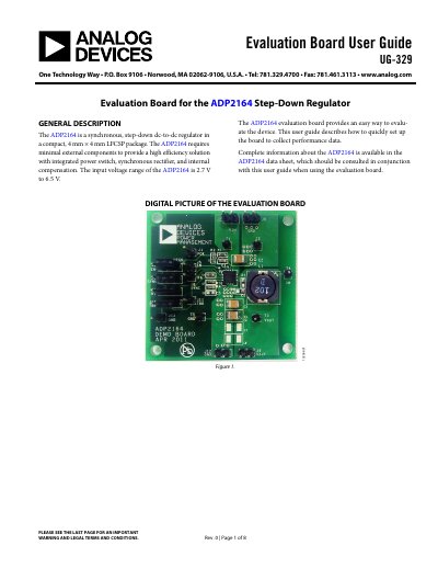
The document provides instructions for setting up the fully assembled and tested ADP2164 evaluation board. It details jumper configurations for enabling output voltage, selecting PWM or external clock synchronization, and adjusting switching frequency via jumpers J7 (RT) and J10 (TRK). The guide also covers proper connections for input power sources, loads, and voltmeters to test points T1 through T5.
| Input Voltage Range | 2.7 V to 6.5 V |
|---|---|
| Package Type | 4 mm × 4 mm LFCSP |
If the input power source is above 2.7 V, the output voltage rises to 1.2 V by default.
Set jumper J7 (RT) to Low.
Set jumper J2 (EN) to High.