
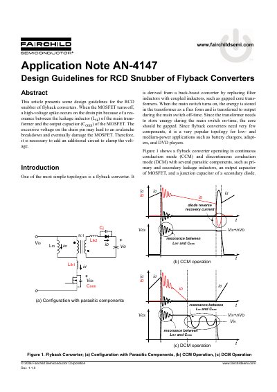
This article presents some design guidelines for the RCD snubber of flyback converters. When the MOSFET turns off, a high-voltage spike occurs on the drain pin because of a resonance between the leakage inductor (Llk) of the main transformer and the output capacitor (COSS) of the MOSFET. The excessive voltage on the drain pin may lead to an avalanche breakdown and eventually damage the MOSFET. Therefore, it is necessary to add an additional circuit to clamp the voltage.
The document explains the causes of excessive voltage on the drain pin of a MOSFET in flyback converters, specifically due to resonance between the transformer's leakage inductance and the MOSFET's output capacitance. It details how an RCD snubber circuit clamps this voltage to prevent avalanche breakdown and device damage.
A high-voltage spike occurs due to resonance between the leakage inductor of the main transformer and the output capacitor of the MOSFET.
In general, a ripple of 5% to 10% is considered reasonable for the snubber circuit.
The voltage rating of the snubber diode should be higher than the rated voltage of the MOSFET (BVggg).