
This document provides assembly guidelines for Fairchild's 6x6 DriverMOS packaging, including information on the packaging technology, circuit design considerations, board mounting, soldering, and back end processing.
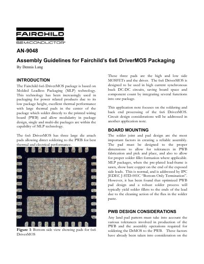
This document provides assembly guidelines for the Fairchild 6x6 DriverMOS package, which utilizes Molded Leadless Packaging (MLP) technology. It focuses on soldering and back-end processing to ensure reliable assembly in high current synchronous buck DC-DC circuits. The guide details requirements for Printed Wiring Board (PWB) design, including pad dimensions and material selection, as well as considerations for using vias within the center pads.
| Peak Reflow Temperature | 260°C |
|---|---|
| Package Lead Finish | NiPdAu |
| Recommended Solder Alloy | SAC 305 |
| Recommended Stencil Thickness | 4 mil |
| Recommended Via Drill Size | 0.3mm |
| Recommended Via Plating | 1 ounce copper |
| Max Recommended Voiding | 25% |
The recommended lead-free solder paste alloy is SAC 305 (96.5 Sn/3.0Au/0.5Cu).
Yes, but users should realize vias often create voiding and should study the process design with x-ray inspection.
Fairchild recommends a guideline of 25% voiding for 6x6 DriverMOS packages.
No, it is recommended that this component not be reused if rework becomes necessary due to high temperatures.