
Introduces the assembly guidelines for Fairchild TinyBuck™ packaging
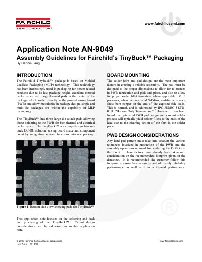
This document outlines assembly guidelines for the Fairchild TinyBuck package, which utilizes Molded Leadless Packaging (MLP) technology. It focuses on soldering and back-end processing to ensure reliable assembly and optimal thermal performance. Key considerations include PWB design, pad finishes, and the use of vias.
| Peak Reflow Temperature | 260°C |
|---|---|
| Recommended Solder Paste Alloy | SAC 305 |
| Recommended Stencil Thickness | 4 mil |
| Recommended Stencil Aperture Coverage | 70% |
| Acceptable Stencil Aperture Coverage Range | 50-80% |
| Recommended Via Drill Size | 0.3mm |
| Maximum Recommended Voiding | 25% |
The recommended lead-free solder paste alloy is SAC 305 (96.5 Sn/3.0Au/0.5Cu).
Fairchild recommends a guideline of 25% voiding for TinyBuck packages.
The TinyBuck package is rated for a peak reflow temperature of 260°C.