
This document describes the “shoot-through” phenomenon in synchronous buck converters and provides two solutions to mitigate it.
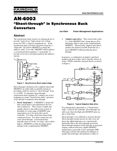
The document discusses the synchronous buck converter circuit, which uses a high-side and a low-side MOSFET to provide power. It defines shoot-through as the condition where both MOSFETs are turned on simultaneously, creating a path for current from the input to ground. This phenomenon can lead to increased ringing, reduced efficiency, higher temperatures, and higher EMI.
The primary cause of shoot-through identified is the 'gate step,' which occurs when the high dv/dt on the switch node couples charge through the MOSFET capacitance, driving the gate voltage positive just as the driver attempts to hold it low. The note analyzes how internal resistances and damping resistors affect this voltage step and provides analytical techniques to predict and reduce shoot-through currents, including the use of Schottky diodes and slowing down the high-side MOSFET rise time.
Placing a Schottky diode across a damping resistor reduces the error in the adaptive gate drive, significantly lowering the peak current and power loss.
Shoot-through manifests as increased ringing, reduced efficiency, higher MOSFET temperatures, and higher EMI.
The theoretical peak current for MOSFET4 is 16.37 A.
The peak current drops from 36 A to 0.29 A when using a Schottky diode.