
NUP4201DR2 is a transient voltage suppressor from Semiconductor Components Industries, LLC. It is designed to protect equipment attached to high speed communication lines from ESD, EFT, and lighting.
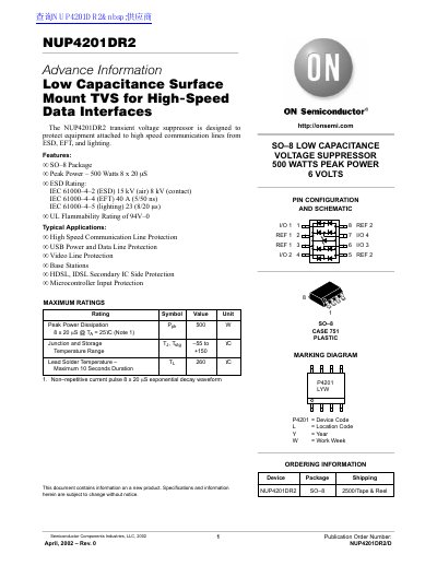
The NUP4201DR2 is a transient voltage suppressor (TVS) device featuring an integrated design of surge-rated steering diodes and a TVS diode in an SO-8 package. It is specifically engineered to protect sensitive electronics, such as communications systems and computer peripherals, against damage from electrostatic discharge (ESD), EFT, and lightning on high-speed communication lines.
The device offers three configuration options for protecting up to four data lines: Option 1 uses the positive supply rail (Vcc) as a reference; Option 2 includes bias and power supply isolation using a recommended 10kΩ resistor; and Option 3 utilizes the internal TVS diode as a reference when no positive supply is available. The document also details 'Rail to Rail' protection topologies, comparing discrete diode configurations with the integrated 'RailClamp' concept.
| Peak Power Dissipation (8 x 20 µs) | 500 W |
|---|---|
| ESD Rating IEC 61000-4—2 (Air) | 15 kV |
| EFT Rating IEC 61000-4—4 | 40 A |
| Lighting Rating IEC 61000-4-5 | 23 kV |
| Reverse Breakdown Voltage (Typical) | 6.0 V |
The device has a peak power dissipation of 500 Watts for an 8 x 20 µs pulse.
In Option 1, the four data lines are connected at pins 1, 4, 6, and 7.