
The MC34063A Series is a monolithic control circuit containing the primary functions required for DC−to−DC converters. These devices consist of an internal temperature compensated reference, comparator, controlled duty cycle oscillator with an active current limit circuit, driver and high current output switch. This series was specifically designed to be incorporated in Step−Down and Step−Up and Voltage−Inverting applications with a minimum number of external components. Refer to Application Notes AN920A/D and AN954/D for additional design information.
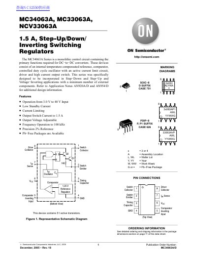
The MC34063A Series is a monolithic control circuit containing the primary functions required for DC-to-DC converters. These devices consist of an internal temperature compensated reference, comparator, controlled duty cycle oscillator with an active current limit circuit, driver and high current output switch. This series was specifically designed to be incorporated in Step-Down and Step-Up and Voltage-Inverting applications with a minimum number of external components.
The document provides detailed electrical characteristics, maximum ratings, and application circuit diagrams for step-up, step-down, and voltage inverting converters. It includes test results for line regulation, load regulation, efficiency, and output ripple under various conditions, as well as package dimensions for SOIC-8 and PDIP-8 packages.
| Output Switch Current | 1.5 A |
|---|---|
| Operating Input Voltage | 3.0 V to 40 V |
| Maximum Power Dissipation (Plastic Package) | 1.25 W |
| Maximum Power Dissipation (SOIC Package) | 625 mW |
| Operating Junction Temperature | +150 °C |
| Oscillator Frequency | 24 to 42 kHz |
| Reference Voltage | 1.25 V |
The device operates from an input voltage of 3.0 V to 40 V.
The output switch current is rated up to 1.5 A.
The typical oscillator frequency is 33 kHz when using a 1.0 nF timing capacitor.