
LMX2505 is a highly integrated, high performance, low power frequency synthesizer system optimized for dual-band Japan PDC mobile handsets. Using a proprietary digi- tal phase locked loop technique, LMX2505 generates very stable, low noise local oscillator signals for up and down conversion in wireless communications devices. LMX2505 includes dual voltage controlled oscillators (VCOs) for the upper and lower Japan PDC frequency bands, a loop filter, and a fractional-N RF PLL based on a delta sigma modulator. In concert these blocks form a closed loop RF synthesizer system. The RF synthesizer system supports two frequency bands: PDC1500 and PDC800. Serial data is transferred to the device via a three-wire MICROWIRE interface (DATA, LE, CLK). Operating supply voltage ranges from 2.5 V to 3.3 V. LMX2505 features low current consumption: 10 mA at 2.8 V when operating in the PDC800 mode. LMX2505 is available in a 28-pin leadless leadframe pack- age (LLP).
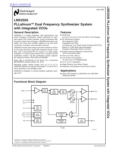
The LMX2505 is a highly integrated, high-performance, low-power frequency synthesizer system optimized for dual-band Japan PDC mobile handsets. It utilizes a proprietary digital phase-locked loop technique to generate stable, low-noise local oscillator signals for up and down conversion in wireless communications devices.
The device includes two voltage-controlled oscillators (VCOs) for the upper and lower Japan PDC frequency bands, an integrated loop filter, and a fractional-N RF PLL based on a delta-sigma modulator. It supports the PDC1500 and PDC800 frequency bands and features low current consumption with operation voltages ranging from 2.5 V to 3.3 V.
| Operating Supply Voltage | 2.5 V to 3.3 V |
|---|---|
| Package Type | 28-pin leadless leadframe package (LLP) |
| Frequency Resolution | Down to 20 kHz |
| Supported Reference Frequencies | 12.6/14.4/25.2/26.0 MHz |
| Phase Noise (@ 25 kHz offset) | -95 to -93 dBc/Hz |
The RF synthesizer system supports two frequency bands: PDC1500 and PDC800.
Serial data is transferred to the device via a three-wire MICROWIRE interface (DATA, LE, CLK).
The supported reference oscillator input frequencies are 12.6/14.4/25.2/26.0 MHz.