
LMP201X is a precision, low noise, low power, no 1/f noise operational amplifier with high open loop gain, voltage gain bandwidth product and output drive capability. It can be used in transducer amplifiers, high gain configurations, ADC buffer amplifiers, DAC I-V conversion and other applications requiring precision and long term stability.
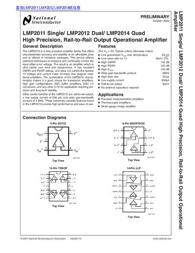
The LMP201X family is a new precision amplifier offering unprecedented accuracy and stability at an affordable price in miniature packages. Utilizing patented techniques to measure and correct input offset error voltage, these devices are ultra-stable over time and temperature. They feature excellent CMRR and PSRR ratings and do not exhibit the familiar 1/f voltage and current noise increase found in traditional amplifiers.
| Input Offset Voltage | 60 pV |
|---|---|
| Supply Current | 930 pA |
| Gain-Bandwidth Product | 3 MHz |
| Slew Rate | 4 V/us |
| Output Swing | 30mV |
The device is a good choice for transducer amplifiers, high gain configurations, ADC buffer amplifiers, and DAC I-V conversion.
No, the LMP201X does not require external capacitors.
The guaranteed input offset voltage over temperature is 60 pV.