
AMD Am25LS2519 Quad Register Datasheet

Query AM25LS2519 supplier
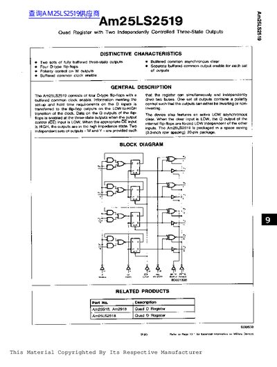

AMD Am25LS2519 Quad Register Datasheet - cover page
Brand
AMD
Category
Other Electronics
Document type
Datasheet
Language
English
Pages
6
File format
PDF
File size
167 KB
Published
11 June, 2012
Updated
30 September, 2023
MD5 checksum
D431656CAB094695E0B3D46C17FE725C

About this manual

The AMD Am25LS2519 is a quad register featuring four D-type flip-flops with buffered common clock enable. It provides two independent sets of fully buffered three-state outputs, labeled W and Y, allowing the device to simultaneously and independently drive two buses. One set of outputs includes a polarity control, enabling the outputs to function as either inverting or non-inverting.

What's inside

  • Distinctive Characteristics
  • General Description
  • Connection Diagram
  • Ordering Information
  • Pin Description
  • Function Table
  • Absolute Maximum Ratings
  • Operating Ranges
  • DC Characteristics
  • Switching Characteristics

Specifications

Number of Flip-FlopsFour
Package Type20-pin
Operating Temperature (Military)-55°C to +125°C
Supply Voltage (Commercial)+4.75V to +5.25V

Frequently asked questions

What is the function of the POL input?

The POL input controls the polarity of the W outputs; when LOW, they are non-inverting, and when HIGH, they are inverting.

How many D-type flip-flops does this register contain?

It contains four D-type flip-flops.

What is the supply voltage range for commercial devices?

The supply voltage ranges from +4.75V to +5.25V.

Download PDF (167 KB)

More AMD Manuals


View all AMD manuals →