
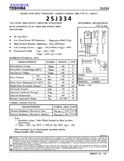
This document is a technical datasheet for the TOSHIBA 2SJ334, a silicon P-channel enhancement-mode field effect transistor. It is designed for high-speed, high-current switching applications such as DC-DC converters, relay drives, and motor drives.
The datasheet provides comprehensive electrical characteristics including maximum ratings like a drain-source voltage of -60V and a continuous drain current of -30A. It also includes detailed graphs illustrating the safe operating area (SOA), transfer characteristics, output characteristics, and thermal performance under various conditions.
| Drain-Source Voltage (Vdss) | -60 V |
|---|---|
| Continuous Drain Current (Idc) | -30 A |
| Pulse Drain Current (Ipp) | -120 A |
| Drain Power Dissipation | 45 W |
| Channel Temperature (Tch) | 150 °C |
| Gate Threshold Voltage (Vth) | -0.8 ~ -2.0 V |
| Drain-Source ON Resistance (RDS(ON)) | 29 mΩ (Typ.) |
| Thermal Resistance, Channel to Case | 2.78 °C/W |
The maximum continuous drain current rating is -30 A.
The maximum drain power dissipation at a case temperature of 25°C is 45 W.
The typical drain-source on resistance under those conditions is 29 mΩ.