
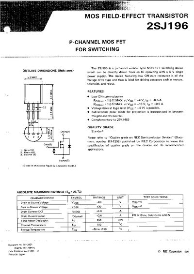
This document is a technical datasheet for the NEC 2SJ196, a p-channel vertical type MOS FET designed for switching applications. The device features low ON-state resistance and can be directly driven from an IC operating with a 5 V single power supply.
Key specifications include a maximum drain current of 1.0 A (DC) and a total power dissipation of 750 mW at Tg = 25 °C. The datasheet provides detailed electrical characteristics, typical performance curves under various conditions, and recommended soldering procedures for assembly.
| Drain Current (DC) | 1.0 A |
|---|---|
| Total Power Dissipation | 750 mW |
| Channel Temperature | 150 °C |
| Drain to Source Voltage | -60 V |
| Gate Cutoff Voltage (Typ.) | -2.1 V |
The maximum drain current (DC) is 1.0 A.
Yes, it can be directly driven from an IC operating with a 5 V single power supply.
For wave soldering, the maximum bath temperature should be 260 °C for no more than 10 seconds.