
MC10EP05/D is an 3.3V / 5V�ECL 2−Input Differential AND/NAND device produced by ON Semiconductor, with a typical propagation delay of 220 ps, a typical maximum frequency of >3 GHz, a PECL mode operating range of VCC = 3.0 V to 5.5 V and VEE = 0 V, a NECL mode operating range of VCC = 0 V and VEE = −3.0 V to −5.5 V, an open input default state, a safety clamp on the inputs, a Q output that will default to low voltage when the inputs are open or at VEE
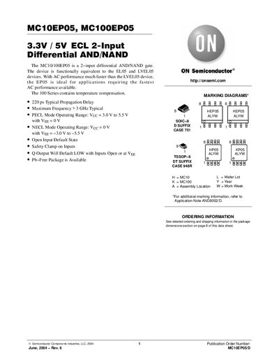
The MC10EP05 and MC100EP05 are 2-input differential AND/NAND gates designed for applications requiring fast AC performance, with the 100 Series offering temperature compensation. The devices are functionally equivalent to the ELO5 and LVELO5 but provide significantly faster speeds.
| Propagation Delay (Typical) | 220 ps |
|---|---|
| Maximum Frequency (Typical) | > 3 GHz |
| PECL Mode Operating Range Vcc | 3.0 V to 5.5 V |
| Operating Temperature Range | -40 to +85 °C |
| Internal Input Pulldown Resistor | 75 kΩ |
| ESD Protection (Human Body Model) | >4kV |
The typical propagation delay is 220 ps.
The device supports a maximum frequency greater than 3 GHz typically.
Yes, the 100 Series contains temperature compensation.
The Q Output will default LOW with Inputs Open or at Vgp.