
CD4049UBC and CD4050BC are six-way inverting buffers/six-way non-inverting buffers, which are specially designed for CMOS to DTL/TTL logic conversion or CMOS current driver. They can directly drive two DTL/TTL loads at VDD=5.0V and have a wide supply voltage range(3.0V-15V), high source and sink current capability, and special input protection that allows input voltage to exceed VDD.
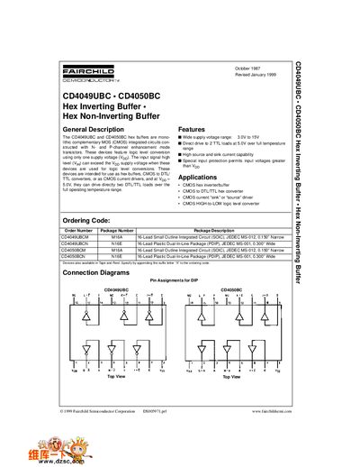
This document provides technical specifications for the CD4049UBC (Hex Inverting Buffer) and CD4050BC (Hex Non-Inverting Buffer), which are monolithic complementary MOS integrated circuits. These devices feature logic level conversion using a single supply voltage, allowing input signal high levels to exceed the supply voltage.
| Supply Voltage Range | 3.0V to 15V |
|---|---|
| Operating Temperature Range | -40°C to +85°C |
| TTL Load Drive Capability | 2 loads at 5.0V |
The devices support a wide supply voltage range from 3.0V to 15V.
Yes, special input protection permits input voltages greater than Vpp.