
This document describes the features and characteristics of the 2SK3113B N-channel MOS FET device, designed for high voltage applications such as switching power supply and AC adapter.
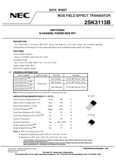
This document is a datasheet for the NEC 2SK3113B, an N-channel MOS field effect transistor designed for high voltage applications such as switching power supplies and AC adapters. The device features low on-state resistance and excellent switching characteristics.
The datasheet provides absolute maximum ratings, electrical characteristics including capacitance and switching times, typical performance curves, and package drawings for TO-251 and TO-252 configurations.
| Drain to Source Voltage (Vds) | 600 V |
|---|---|
| Gate to Source Voltage (Vgs) | +30 V |
| Drain Current (DC) | +2.0 A |
| Total Power Dissipation (Ta = 25°C) | 1.0 W |
| Channel Temperature | 150 °C |
| Storage Temperature | -55 to +150 °C |
It is designed for high voltage applications such as switching power supply and AC adapter.
The device supports a DC drain current of +2.0 A and a total power dissipation of 20 W at a case temperature of 25°C.
The absolute maximum drain-to-source voltage is rated at 600 V.
The typical total gate charge is 7.9 nC, and the maximum drain-to-source on-state resistance is 4.4 Ω.