
The CDC2516 is a 3.3V phase-lock loop clock driver for synchronous DRAM applications. It distributes one clock input to four banks of four outputs, with separate output enable for each output bank. The external feedback pin (FBIN) is used to synchronize the outputs to the clock input. The CDC2516 has integrated series-damping resistors on-chip and does not require an external RC network. It operates at 3.3V VCC and is packaged in a plastic 48-pin thin shrink small-outline package.
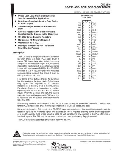
The CDC2516 is a high-performance, low-skew, low-jitter phase-lock loop (PLL) clock driver specifically designed for use with synchronous DRAMs. It distributes one clock input to four banks of four outputs, providing 16 copies of the input clock signal.
Unlike many other PLL products, the CDC2516 does not require external RC networks because its loop filter is included on-chip. The device operates at a supply voltage (Voc) of 3.3 V and features integrated series-damping resistors to drive point-to-point loads effectively.
| Supply Voltage (Voc) | 3 V to 3.6 V |
|---|---|
| Operating Temperature Range | 0°C to 70°C |
| Clock Frequency (fclk) | 25 MHz to 125 MHz |
| Output Current (High Level) | -12 mA |
| Output Current (Low Level) | -12 mA |
| Stabilization Time | 7 ms |
No, unlike many products containing PLLs, the CDC2516 does not require external RC networks because its loop filter is included on-chip.
The device operates at a 3.3-V Voc with a recommended range of 3 V to 3.6 V.
It provides four banks of four outputs, totaling 16 low-skew copies of the input clock.