
MN54F189-X REV 1A0 is a 64-bit random access memory with 3-state outputs. The memory is organized as a 16-word by 4-bit array, address inputs are buffered to minimize loading and are fully decoded on-chip. Outputs are 3-state and are in the high impedance state whenever the Chip Select (CS) input is HIGH. Outputs are active only in the Read mode and the output data is the complement of the stored data.
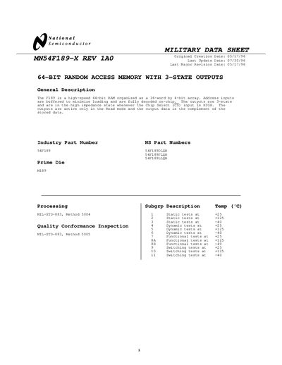
This document is a military data sheet for the National Semiconductor MN54F189-X, a high-speed 64-bit Random Access Memory (RAM) organized as a 16-word by 4-bit array. The device features 3-state outputs suitable for data bus applications and buffered address inputs to minimize loading.
The datasheet provides absolute maximum ratings, recommended operating conditions, and detailed electrical characteristics including DC parameters such as input/output currents and voltages, and AC timing parameters like access time and setup/hold times across commercial and military temperature ranges.
| Organization | 16-word by 4-bit array |
|---|---|
| Data Width | 64-bit |
| Supply Voltage (Military) | +4.5V to +5.5V |
| Operating Temperature Range (Military) | -40°C to +125°C |
It is organized as a 16-word by 4-bit array.
The recommended operating supply voltage is +4.5V to +5.5V.
Yes, address inputs are buffered to minimize loading.