
BD3539FVM/NUX is a termination regulator compatible with JEDEC DDR1-SDRAM, DDR2-SDRAM, DDR3-SDRAM which functions as a linear power supply incorporating an N-channel MOSFET and provides a sink/source current capability up to 1A respectively.
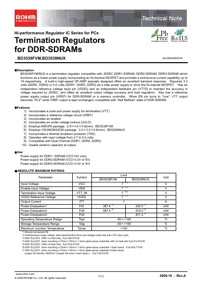
The BD3539FVM (and BD3539NUX) is a high‑performance termination regulator for DDR‑SDRAM applications. It integrates a push‑pull power supply, reference voltage circuit, enable control, UVLO protection and a thermal shutdown circuit, delivering up to 1 A sink/source current.
The document provides a detailed description, absolute maximum ratings, operating conditions, electrical characteristics, pin‑out tables, evaluation‑board schematics, layout recommendations, and ordering information, helping designers implement the device safely and efficiently.
| Input voltage (VCC) range | 2.7 V – 5.5 V |
|---|---|
| Termination input voltage (VTT_IN) range | 1.0 V – 5.5 V |
| Reference voltage (VDDQ) range | 1.0 V – 2.75 V |
| Enable input voltage (VEN) range | -0.3 V – 5.5 V |
| UVLO threshold voltage (VUVLO) | 2.30 V – 2.60 V |
| Maximum power dissipation (Pd1) | 387.4 mW |
VCC may be between 2.7 V and 5.5 V, while VTT_IN may be between 1.0 V and 5.5 V.
VTTS has relatively high impedance, so its trace should be kept short and placed on an upper layer with minimal stray capacitance.