
BD3538F / HFN is a termination regulator compatible with JEDEC DDR-SDRAM, which functions as a linear power supply incorporating an N-channel MOSFET and provides a sink / source current capability up to 1A respectively. A built-in high-speed OP-AMP specially designed offers an excellent transient response. Requires 3.3 volts or 5.0 volts as a bias power supply to drive the N-channel MOSFET. Has an independent reference voltage input pin (VDDQ) and an independent feedback pin (VTTS) to maintain the accuracy in voltage required by JEDEC, and offers an excellent output voltage accuracy and load regulation. Also has a reference power supply output pin (VREF) for DDR-SDRAM or a memory controller. When EN pin turns to “Low”, VTT output becomes “Hi-Z” while VREF output is kept unchanged, compatible with “Self Refresh” state of DDR-SDRAM.
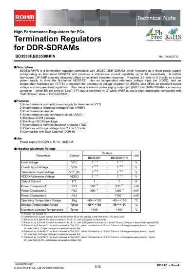
The ROHM BD3538F (and BD3538HFN) is a high‑performance termination regulator for DDR‑SDRAM applications. It integrates an N‑channel MOSFET, a high‑speed op‑amp, and provides up to 1 A sink/source current, with independent VDDQ, VREF and VTT pins for precise voltage control.
The document includes a description of operation, absolute maximum ratings, electrical characteristics, pin configuration, an evaluation‑board schematic, and ordering information. It also offers notes on thermal design, EMI considerations, and recommended external components such as capacitors and resistors.
| Input Voltage (VCC) range | 2.7 V – 5.5 V |
|---|---|
| Termination Input Voltage (VTT_IN) range | 1.0 V – 5.5 V |
| VDDQ Reference Voltage range | 1.0 V – 2.75 V |
| Enable Input Voltage (VEN) range | -0.3 V – 5.5 V |
| Maximum sink/source current (ITT) | ±1.0 A |
| Power Dissipation (Pdi) | 560 mW |
| Operating Temperature Range | -40 °C – +105 °C |
| Package types | SOP8, HSON8 |
The device operates with VCC between 2.7 V and 5.5 V.
The VTT output can source or sink up to 1.0 A.
The part is offered in SOP8 and HSON8 packages.
When EN is high (≥2.3 V) VTT output is enabled; when EN is low (≤0.8 V) VTT is turned off (Hi‑Z) while VREF remains active.