
This document provides technical information to properly design a JTAG emulator interface for Analog Devices, Inc. (ADI) processor targets
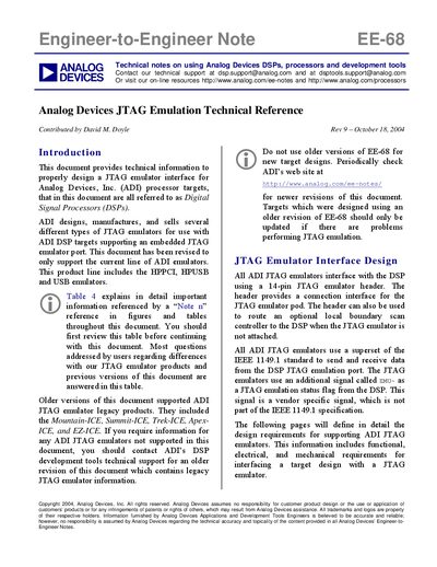
The EE-68 Engineer‑to‑Engineer Note describes how to design a JTAG emulator interface for Analog Devices DSPs. It covers the current HPPCI, HPUSB and USB JTAG emulators, their 14‑pin header, signal definitions, and the optional local boundary‑scan controller.
The document also details mechanical clearances, pod dimensions, PCB layout recommendations, power‑up sequencing, and electrical specifications such as voltage‑sense capability and supported JTAG I/O voltage levels.
| Header pin count | 14 pins |
|---|---|
| Header spacing | 0.1" x 0.1" |
| Minimum post length | 0.235" |
| Header clearance | at least 0.30" length and 0.10" width |
| Pod voltage tolerance | up to SVDC |
| Supported JTAG VO voltages | 5 V, 3.3 V, 2.5 V, 1.8 V |
The current line includes the HPPCI, HPUSB and USB emulators.
A minimum clearance of 0.30" around the length and 0.10" around the width of the header is required.
The JTAG emulator should be powered on and connected to the host PC before attaching it to the target header.