
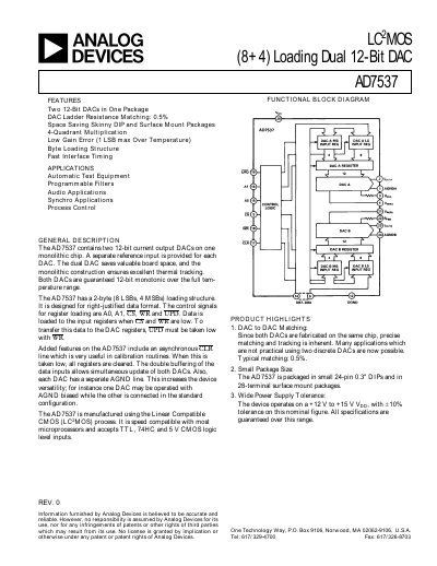
The AD7537 contains two 12-bit current-output DACs on one monolithic chip, with a separate reference input for each DAC. It uses a 2-byte loading structure for right-justified data and provides control signals A0, A1, CS, WR and UPD, plus an asynchronous CLR line and double buffering for simultaneous DAC updates.
The device is manufactured using the Linear Compatible CMOS process and accepts TTL, 74HC and 5 V CMOS logic-level inputs. It is packaged in 24-pin 0.3-inch DIPs and 28-terminal surface-mount packages, and operates on a +12 V to +15 V VDD supply with +10% tolerance.
| Resolution | 12 bits |
|---|---|
| Number of DACs | Two 12-bit DACs |
| DAC ladder resistance matching | 0.5% |
| Gain error | 1 LSB max over temperature |
| Supply voltage | +12 V to +15 V; ±10% tolerance |
| Digital input compatibility | TTL, 74HC and 5 V CMOS |
| Packages | 24-pin 0.3-inch DIP and 28-terminal surface mount |
The AD7537 contains two 12-bit current-output DACs on one monolithic chip.
It uses a 2-byte loading structure for right-justified data.
It operates on a +12 V to +15 V VDD supply with +10% tolerance.
It accepts TTL, 74HC and 5 V CMOS logic-level inputs.