
This document describes a precision analog microcontroller ARM7TDMI MCU with 12-bit ADC and DDS DAC. The product features a multichannel, 12-bit, 1 MSPS ADC with up to 14 ADC channels, fully differential and single-ended modes, 0 to VREF analog input range; a 10-bit DAC; a 32-bit 21 MHz direct digital synthesis (DDS); current-to-voltage (I/V) conversion; an integrated second-order low-pass filter (LPF); DDS input to DAC; a 100 Ω line driver; an on-chip voltage reference; an on-chip temperature sensor (±3°C); a voltage comparator; a microcontroller ARM7TDMI core with 16-/32-bit RISC architecture; a JTAG port that supports code download and debug; an external watch crystal/clock source; a 41.78 MHz PLL with 8-way programmable divider; an optional trimmed on-chip oscillator; 126 kB Flash/EE memory, 8 kB SRAM; and in-circuit download, JTAG-based.
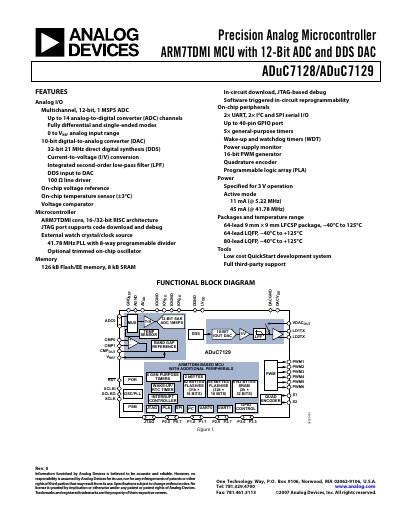
The ADuC7128/ADuC7129 are fully integrated 12‑bit, 1 MSPS data‑acquisition microcontrollers that combine an ARM7TDMI core, multi‑channel ADC, DDS‑based DAC, and on‑chip Flash/EE memory. The document details the device architecture, pin functions, and electrical characteristics.
Key sections cover functional block diagrams, timing specifications, power‑supply monitoring, peripheral interfaces (UART, SPI, I²C, PWM, quadrature encoder), memory organization, and development tools. The handbook also includes design recommendations, ordering information, and mechanical dimensions.
| ADC resolution | 12 bits |
|---|---|
| Core clock frequency | 41.78 MHz |
| Flash/EE memory size | 126 kB |
| SRAM size | 8 kB |
| Supply voltage range | 3.0 V to 3.6 V |
| Operating temperature range | -40 °C to +125 °C |
| Number of ADC channels | Up to 14 |
| Active‑mode current consumption (41.78 MHz) | 45 mA |
The internal PLL generates a 41.78 MHz clock that can be divided to produce the MCU core clock.
The microcontroller includes up to 14 single‑ended ADC channels, usable in differential or single‑ended mode.
The device contains 126 kB of non‑volatile Flash/EE memory.
The parts operate from 3.0 V to 3.6 V.