
This document provides the GFB70N03 datasheet, including specifications, characteristics curves, and package dimensions.
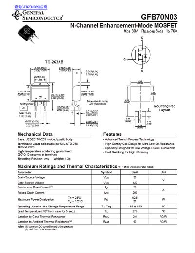
The GFB70N03 is an N‑Channel enhancement‑mode MOSFET packaged in a JEDEC TO‑263AB molded plastic body. It features an advanced trench process, high‑density cell design for ultra‑low on‑resistance, and is suitable for low‑voltage DC/DC converters with fast switching and high efficiency.
The document lists detailed electrical characteristics, maximum ratings, and thermal data, including drain‑source voltage, continuous and pulsed drain currents, on‑resistance versus temperature, and gate charge curves. Characteristic curves illustrate performance across voltage, current, and temperature ranges.
| Drain‑Source Voltage (VDS) | 30 V |
|---|---|
| Gate‑Source Voltage (VGS) | 20 V |
| Continuous Drain Current (ID) | 70 A |
| Pulsed Drain Current (IDM) | 200 A |
| Junction‑to‑Case Thermal Resistance (RJC) | 2.0 °C/W |
| Junction‑to‑Ambient Thermal Resistance (RJA) | 40 °C/W |
The GFB70N03 is rated for a maximum drain‑source voltage of 30 V.
The device can continuously conduct up to 70 A of drain current.
The junction‑to‑case thermal resistance is 2.0 °C/W.