
The MC74LVXT4066 is a high-performance bilateral switch/multiplexer/demultiplexer that utilizes silicon-gate CMOS technology to achieve fast propagation delays, low ON resistances, and low OFF-channel leakage current. It controls analog and digital voltages that may vary across the full power-supply range (from VCC to GND). The LVXT4066 is identical in pinout to the metal-gate CMOS MC14066 and the high-speed CMOS HC4066A. Each device has four independent switches. The device has been designed so that the ON resistances (RON) are much more linear over input voltage than RON of metal-gate CMOS analog switches. The ON/OFF control inputs are compatible with standard LSTTL outputs. The input protection circuitry on this device allows overvoltage tolerance on the ON/OFF control inputs, allowing the device to be used as a logic-level translator from 3.0V CMOS logic to 5.0V CMOS Logic or from 1.8V CMOS logic to 3.0V CMOS Logic while operating at the higher-voltage power supply. The MC74LVXT4066 input structure provides protection when voltages up to 7V are applied, regardless of the supply voltage. This allows the MC74LVXT4066 to be used to interface 5V circuits to 3V circuits.
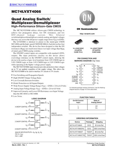
The MC74LVXT4066 quad analog switch/multiplexer uses silicon‑gate CMOS technology to provide fast propagation, low ON resistance, and low OFF‑channel leakage. It supports analog and digital voltages across a 2.0 V to 6.0 V supply range and includes input protection for up to 7 V.
The device is offered in 14‑lead SOIC and 14‑lead TSSOP packages, with detailed electrical characteristics, maximum ratings, and application guidelines provided for designers.
| Supply Voltage Range | 2.0 V to 6.0 V |
|---|---|
| Analog Input Voltage Range | 2.0 V to 6.0 V |
| Maximum Power Dissipation (SOIC) | 500 mW |
| Maximum Input Leakage Current | 5.5 µA |
| ON Resistance (typical at VCC=2.0 V, 25 °C) | ≈250 Ω |
The device operates with a supply voltage from 2.0 V up to 6.0 V.
The SOIC package can dissipate up to 500 mW in still air.
The maximum input leakage current is 5.5 µA.