
This document introduces the features of ADDI7100, including 45MHz correlated double sampler (CDS), 10-bit variable gain amplifier (VGA), low noise optical black clamp circuit, pre-blanking function, 12-bit, 45MHz ADC, 3-wire serial digital interface, 3V single-supply operation, space-saving 32-lead, 5mm×5mm LFCSP.
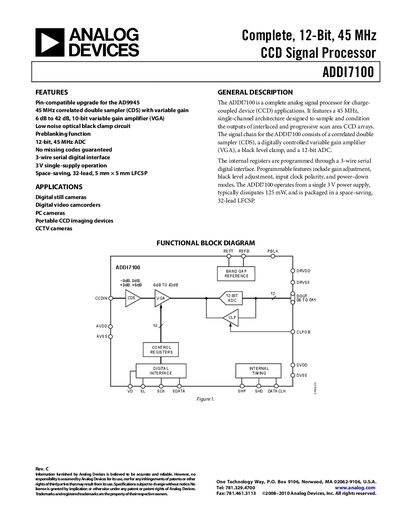
The ADDI7100 is a complete analog signal processor for CCD applications. It integrates a correlated double sampler, a digitally controlled variable‑gain amplifier, a black‑level clamp, and a 12‑bit ADC, all powered from a single 3 V supply. The device is pin‑compatible with the AD9945 and is offered in a compact 32‑lead LFCSP package.
Key features include a 45 MHz sampling rate, programmable gain from 6 dB to 42 dB, a 3‑wire serial digital interface for register programming, low‑noise optical black clamp, and low power consumption (125 mW normal operation). The datasheet provides full specifications, timing diagrams, pin descriptions, and ordering information.
| Operating Temperature Range | -25 °C to +85 °C |
|---|---|
| Power Consumption (Normal Operation) | 125 mW |
| Maximum Clock Rate | 45 MHz |
| ADC Resolution | 12 bits |
| Differential Nonlinearity (DNL) | -1.0 to +0.5 LSB |
| Missing Codes | No missing codes guaranteed |
| Full‑Scale Input Voltage | 2.0 V |
| Reference Top Voltage (REFT) | 2.0 V |
| Reference Bottom Voltage (REFB) | 1.0 V |
| High Level Input Voltage (VIN) | 2.1 V |
| Low Level Input Voltage (VIT) | 0.6 V |
| Package Type | 32‑Lead LFCSP (5 mm × 5 mm) |
The device operates from –25 °C to +85 °C.
Normal operation power consumption is 125 mW.
Registers are programmed via a 3‑wire serial digital interface.
It is supplied in a 32‑lead lead‑frame chip‑scale package (LFCSP) measuring 5 mm × 5 mm.