
The AD5641 is a single, 14-bit, buffered, voltage-out DAC that operates from a 2.7 V to 5.5 V supply and draws a maximum of 100 µA at 5 V. The device features guaranteed monotonicity, power-down, low power serial interface, on-chip output buffer amplifier, rail-to-rail operation, and SYNC interrupt facility. It is widely used in voltage level setting, portable battery-powered instruments, digital gain and offset adjustment, programmable voltage and current sources, and programmable attenuators.
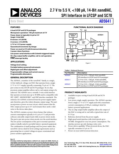
The AD5641 nanoDAC is a single‑channel, 14‑bit buffered voltage‑output DAC that operates from a single 2.7 V to 5.5 V supply. It consumes as little as 75 µA at 5 V in normal mode and can be powered down to 0.2 µA at 3 V, making it suitable for battery‑powered instruments and space‑constrained applications. The device is offered in 6‑lead LFCSP and SC70 packages and includes an on‑chip rail‑to‑rail output buffer.
A versatile 3‑wire serial interface supports SPI, QSPI™, MICROWIRE™ and DSP standards up to 30 MHz. The AD5641 features power‑on reset to 0 V, brown‑out detection, three power‑down modes, and a SYNC interrupt for precise timing control. Detailed specifications, timing diagrams, pin descriptions, and layout recommendations are provided throughout the sheet.
| Resolution | 14 bits |
|---|---|
| Supply Voltage Range | 2.7 V to 5.5 V |
| Typical Power Consumption (Normal Mode) | 75 µA at 5 V |
| Power‑Down Current | 0.2 µA at 3 V |
| Maximum Clock Frequency | 30 MHz |
| Output Voltage Range | 0 V to VDD |
| Slew Rate | 0.5 V/µs |
| Package Options | 6‑lead LFCSP and SC70 |
| Operating Temperature Range | -40 °C to +125 °C |
The AD5641 operates from a single supply of 2.7 V to 5.5 V.
In normal mode it typically draws 75 µA at a 5 V supply.
The serial interface can run up to 30 MHz.
The device is offered in 6‑lead LFCSP and SC70 packages, each with six pins.