
The document describes the features and characteristics of the AD5390/AD5391/AD5392 series products, including the number of channels, voltage output resolution, INL accuracy, reference voltage, operating temperature range, and package types.
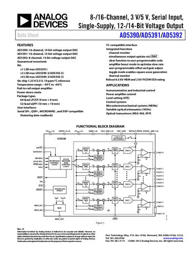
The AD5390, AD5391 and AD5392 are single‑supply, multi‑channel DACs offering 16‑channel (AD5390/AD5391) or 8‑channel (AD5392) configurations with 14‑bit or 12‑bit resolution. They are available in 64‑lead LFCSP (9 mm × 9 mm) or 52‑lead LQFP (10 mm × 10 mm) packages and include an on‑chip reference, output amplifier, and channel monitor.
These devices feature a 3‑wire serial interface compatible with SPI, QSPI, MICROWIRE, DSP and I²C standards, support simultaneous output updates via LDAC, and operate over a temperature range of –40 °C to +85 °C. Typical power consumption is 0.25 mA per channel, and they are suited for instrumentation, industrial control, power‑amplifier control, and optical communication applications.
| Resolution | 14‑bit (AD5390) / 12‑bit (AD5391) |
|---|---|
| Relative Accuracy | +3 LSB max (AD5390‑5) / +1 LSB max (AD5391‑5) |
| Output Voltage Range (AVpp) | 4.5 V to 5.5 V |
| Power Consumption per Channel | 0.25 mA typical |
| Operating Temperature Range | –40 °C to +85 °C |
| Package Options | 64‑lead LFCSP (9 mm × 9 mm) and 52‑lead LQFP (10 mm × 10 mm) |
It supports SPI, QSPI, MICROWIRE, DSP‑compatible, and I²C‑compatible serial interfaces.
Typical power consumption is 0.25 mA per channel.
The device operates from –40 °C to +85 °C.
It is offered in a 64‑lead LFCSP (9 mm × 9 mm) and a 52‑lead LQFP (10 mm × 10 mm).