
The AD5061 is a single channel 16-bit buffered voltage output DAC with a supply voltage range of 2.7 V to 5.5 V in a SOT-23 package. The device offers ±4 LSB of relative accuracy and guaranteed monotonicity with a ±1 LSB DNL specification. The AD5061 uses a 3-wire serial interface that operates at clock frequencies up to 30 MHz and is compatible with standard SPI, QSPI, MICROWIRE, and DSP interface standards. The AD5061's external reference voltage is provided by the VREF pin. A reference buffer is also provided on-chip. The device also incorporates a power-on reset circuit that ensures that the DAC output is at the midscale level when the VREF pin voltage is 0 V and at the zero level when the VREF pin voltage is 2.5 V.
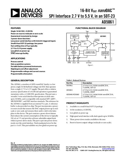
The AD5061 nanoDAC from Analog Devices provides a single 16‑bit buffered voltage‑output DAC in a compact 8‑lead SOT‑23 package. It operates from a 2.7 V to 5.5 V supply, offers low‑power serial interfaces compatible with SPI, QSPI, MICROWIRE and DSP standards, and includes three selectable power‑down functions.
The datasheet lists detailed specifications such as 16‑bit resolution, ±4 LSB INL, 30 MHz maximum serial clock, and typical 330 nA power‑down current. It also covers functional block diagrams, timing characteristics, pin descriptions, typical performance graphs, and guidelines for galvanic isolation, power‑supply bypassing, and board layout.
| Resolution | 16 Bits |
|---|---|
| Power‑supply range | 2.7 V to 5.5 V |
| Maximum serial clock frequency | 30 MHz |
The AD5061 operates from 2.7 V to 5.5 V.
The device supports a serial clock up to 30 MHz.
The AD5061 offers three selectable power‑down modes.
It provides a 16‑bit resolution.