
This is a 32-channel, 14-bit DAC with programmable 50 V to 200 V full-scale output voltage.
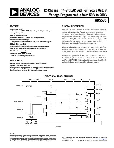
The AD5535 is a highly integrated 32‑channel, 14‑bit digital‑to‑analog converter with an on‑chip high‑voltage output amplifier. The output voltage range is programmable via the REF_IN pin, allowing 0 V‑50 V (REF_IN = 1 V) or 0 V‑200 V (REF_IN = 4 V). Each channel can source 700 µA, making it suitable for optical MEMS mirrors, cross‑point switches and piezoelectric micro‑positioning.
The device operates from standard analog supplies (AVCC ≈ 5 V, DVCC ≈ 2.7‑5.25 V) and a high‑voltage VPP supply up to 210 V. A 3‑wire serial interface supports up to 30 MHz clock rates, with a 1.2 MHz channel‑update rate. The datasheet includes functional block diagrams, pin descriptions, timing characteristics, absolute maximum ratings, typical performance graphs, PCB layout guidelines, and power‑supply sequencing recommendations.
| Resolution | 14 bits |
|---|---|
| Integral Nonlinearity (INL) | ±0.1 % of FSR |
| Differential Nonlinearity (DNL) | –1 LSB to +1 LSB |
| Output Drive Capability | 700 µA per channel |
| Programmable Output Voltage Range | 0 V‑50 V (REF_IN = 1 V) or 0 V‑200 V (REF_IN = 4 V) |
| Channel Update Rate | 1.2 MHz |
| Serial Interface Clock Frequency | up to 30 MHz |
| Power Supply Currents (IPP) | 75‑100 µA per channel |
| Operating Temperature Range | –10 °C to +85 °C |
The output can be programmed from 0 V to 50 V when REF_IN is 1 V, or from 0 V to 200 V when REF_IN is 4 V.
The serial interface supports clock frequencies up to 30 MHz.
Each output amplifier can source up to 700 µA.
The AD5535 operates from –10 °C to +85 °C.