
TD350 is an advanced gate driver for IGBT and power MOSFET. Control and protection functions are included and allow the design of high reliability systems. Innovative active Miller clamp function avoids the need of negative gate drive in most applications and allows the use of a simple bootstrap supply for the high side driver TD350 includes a two-level turn-off feature with adjustable level and delay. This function protects against excessive overvoltage at turn-off in case of overcurrent or short-circuit condition. Same delay is applied at turn-on to prevent pulse width distortion. TD350 also includes an IGBT desaturation protection and a FAULT status output. TD350 is compatible with both pulse transformer and optocoupler signals.
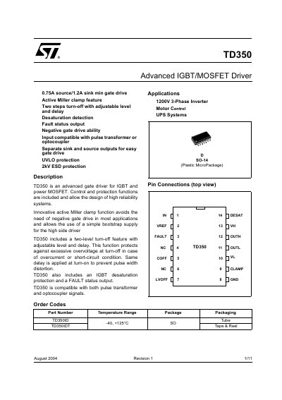
This handbook describes the TD350 advanced gate driver for IGBT and power MOSFET devices. It covers functional blocks, pin descriptions, electrical characteristics, protection features such as active Miller clamp, two‑level turn‑off, desaturation detection, UVLO, and 2 kV ESD protection.
The document includes absolute maximum ratings, typical performance curves, timing diagrams, mechanical package data, and revision history, providing engineers with the information needed to design reliable high‑power inverter and motor‑control systems.
| Maximum Supply Voltage (VH‑VL) | 28 V |
|---|---|
| Operating Temperature Range | -40 to 125 °C |
| Maximum Junction Temperature | 150 °C |
| Typical Output Current (source) | 10 mA |
| UVLO Top Threshold | 10‑12 V |
A capacitor between 10 nF and 100 nF is recommended.
The minimum input pulse width is 100 ns (typical) to 135 ns (minimum).