
The MJ13333 is a Motorola designed high voltage, high-speed, power switching transistor for inductive circuits where fall time is critical. It is particularly suited for line operated switchmode applications such as: Switching Regulators, Inverters, Solenoid and Relay Drivers, Motor Controls and Deflection Circuits.
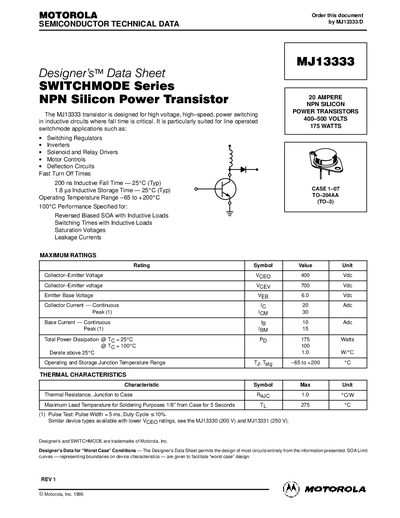
The MJ13333 is a high‑voltage, high‑speed NPN silicon power transistor designed for switch‑mode applications such as regulators, inverters and motor controls. It offers 400 V collector‑emitter voltage, 20 A continuous collector current and 175 W power dissipation.
The datasheet provides detailed electrical specifications, thermal limits, switching performance, safe operating area curves and mechanical dimensions for the TO‑204AA (TO‑3) package, along with test conditions and application notes.
| Collector‑Emitter Voltage (VCEO) | 400 V |
|---|---|
| Collector‑Emitter Voltage (Clamped) (VCE(sus)) | 400 V |
| Collector Current (Continuous) | 20 A |
| Peak Collector Current | 30 A |
| Total Power Dissipation (25 °C) | 175 W |
| Operating Temperature Range | -65 °C to +200 °C |
| Thermal Resistance, Junction‑to‑Case | 1.0 °C/W |
| Inductive Fall Time (typical) | 200 ns |
The MJ13333 is rated for a maximum collector‑emitter voltage of 400 V.
It can handle a continuous collector current of 20 A.
The typical inductive fall time is 200 ns at 25 °C.
The transistor is supplied in a TO‑204AA (TO‑3) package.