
Introducing the features and characteristics of a certain high voltage MOSFET.
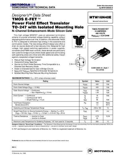
The MTW16N40E is a N‑channel enhancement‑mode power MOSFET designed for high‑voltage, high‑speed switching applications such as power supplies, converters, and PWM motor controls. It features a robust 400 V drain‑source rating, 16 A continuous drain current, and an isolated mounting hole in a TO‑247 package.
The datasheet provides maximum ratings, typical electrical characteristics, safe operating area curves, and thermal data. Package dimensions and mechanical tolerances are listed, and a disclaimer outlines usage limits and liability.
| Drain‑Source Voltage (VDS) | 400 V |
|---|---|
| Continuous Drain Current (ID) | 16 A |
| Gate‑Source Voltage (VGS) Continuous | +20 V |
| Total Power Dissipation (Pp) | 180 W |
| Junction‑to‑Case Thermal Resistance (RθJC) | 0.70 °C·W |
| Junction‑to‑Ambient Thermal Resistance (RθJA) | 40 °C·W |
| Static Drain‑Source On‑Resistance (RDS(on)) Typical | 0.225 Ω |
| Single‑Pulse Drain Current (IDM) | 56 A |
| Avalanche Energy (EAS) at 25 °C | 870 mJ |
| Package Type | TO‑247 with isolated mounting hole |
The MTW16N40E is rated for a maximum drain‑source voltage of 400 V.
It can conduct up to 16 A continuously.
The typical static on‑resistance is 0.225 Ω.
The maximum power dissipation is 180 W.