
This document describes the features and characteristics of the AD8651/AD8652 low noise CMOS amplifiers, including 50 MHz bandwidth, low noise, low distortion, 4.5 nV/√Hz noise, 100 µV offset voltage, 1 pA input bias current, etc.
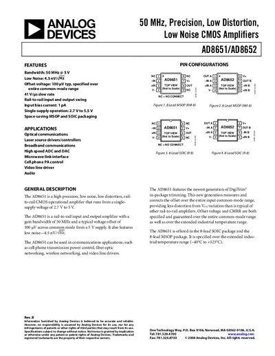
The AD8651/AD8652 amplifiers provide high precision, low distortion, and rail‑to‑rail input and output operation from a single supply of 2.7 V to 5.5 V. They are suited for optical communications, laser drivers, high‑speed ADC/DAC interfaces, microwave links, cell‑phone PA control, video line drivers, and audio applications.
Key features include a 50 MHz gain‑bandwidth product, 4.5 nV/√Hz voltage noise density, 1 pA input bias current, 41 V/µs slew rate, and up to 40 mA output current. The devices are offered in 8‑lead MSOP and SOIC packages and are specified over an extended temperature range of –40 °C to +125 °C.
| Bandwidth | 50 MHz @ 5 V |
|---|---|
| Voltage Noise Density | 4.5 nV/√Hz |
| Input Bias Current | 1 pA |
| Slew Rate | 41 V/µs |
| Supply Voltage Range | 2.7 V to 5.5 V |
| Output Current | 40 mA |
The AD8651 has a gain‑bandwidth product of 50 MHz at a 5 V supply.
Both devices operate from a single supply between 2.7 V and 5.5 V.
The typical input bias current is 1 pA.
The AD8651 exhibits a voltage noise density of 4.5 nV/√Hz.