
AD8551/AD8552/AD8554 is a zero-drift, single-supply, rail-to-rail input/output operational amplifier. Its features include low offset voltage, low input offset drift, wide input and output swing, single-supply operation, high gain, and common mode rejection ratio.
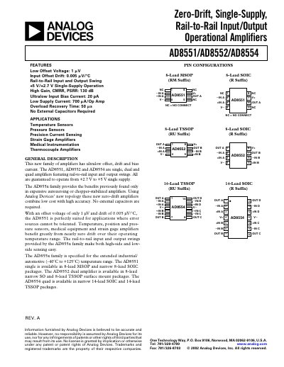
The AD855x family provides ultra‑low offset voltage (as low as 0 µV), low drift (0.005 µV/°C), and low input bias current (typical 20 pA). They operate from a single supply of +2.7 V to +5 V and are specified for an extended industrial/automotive temperature range of –40 °C to +125 °C. These amplifiers are suited for precision sensor interfaces, medical instrumentation, and thermocouple amplification.
The datasheet includes detailed electrical characteristics, ordering information, absolute maximum ratings, and functional description of the auto‑zero architecture. It also provides application notes such as high‑side and low‑side load‑current monitoring circuits.
| Offset Voltage (typical) | 0 µV |
|---|---|
| Input Bias Current (typical) | 20 pA |
| Supply Current per Amplifier (typical) | 850 µA |
| Gain‑Bandwidth Product | 1.5 MHz |
| Power‑Supply Rejection Ratio (typical) | 120 dB |
| Short‑Circuit Current Limit | ±25 mA (±50 mA max) |
The typical offset voltage is 0 µV.
It can operate from a single supply of +2.7 V to +5 V.
The short‑circuit limit is ±25 mA (±50 mA maximum).
Typical supply current is 850 µA per amplifier.