
The ADC12L030 family is a 12-bit plus sign successive approximation A/D converter with serial I/O and configurable input multiplexers. These devices are fully tested with a single 3.3V power supply. The ADC12L032, ADC12L034 and ADC12L038 have 2, 4 and 8 channel multiplexers, respectively. Differential multiplexer outputs and A/D inputs are available on the MUXOUT1, MUXOUT2, A/DIN1 and A/DIN2 pins. The ADC12L030 has a two channel multiplexer with the multiplexer outputs and A/D inputs internally connected. On request, these A/Ds go through a self calibration process that adjusts linearity, zero and full-scale errors to less than ±1⁄2 LSB each. The analog inputs can be configured to operate in various combinations of single-ended, differential, or pseudo-differential modes. A fully differential unipolar analog input range (0V to +3.3V) can be accommodated with a single +3.3V supply. In the differential modes, valid outputs are obtained even when the negative inputs are greater than the positive because of the 12-bit plus sign two’s compliment output data format. The serial I/O is configured to comply with NSC’s MICROWIRE™ and Motorola’s SPI standards. For voltage references, see the LM4040 or LM4041 data sheets.
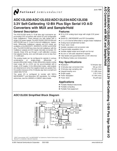
The ADC12L030/ADC12L032/ADC12L034/ADC12L038 family are 12‑bit plus‑sign successive‑approximation A/D converters that operate from a single 3.3 V supply. They provide configurable single‑ended, differential or pseudo‑differential inputs and include on‑chip multiplexers of 2, 4 or 8 channels depending on the model.
Key features include self‑calibration that reduces linearity, zero and full‑scale errors to less than ±1 LSB, serial I/O compatible with Microwire™ and SPI, power‑down mode, programmable acquisition time, and a wide operating temperature range of –40 °C to +85 °C. The datasheet supplies detailed pin descriptions, absolute maximum ratings, electrical characteristics, and mechanical dimensions.
| Resolution | 12‑bit plus sign |
|---|---|
| Conversion time (12‑bit) | 8.8 µs (min) |
| Maximum sampling rate | 73 kHz |
| Supply voltage | 3.3 V ±10 % |
| Power dissipation | 15 mW (max) |
| Power‑down current | 40 µW (typ) |
| Integral linearity error | +1 LSB (max) |
| Input voltage range | 0 V to +3.3 V |
| Operating temperature range | -40 °C to +85 °C |
The minimum conversion time for 12‑bit plus‑sign mode is 8.8 µs.
The device operates from a single 3.3 V supply with a tolerance of ±10 %.
ADC12L030 has a 2‑channel MUX, ADC12L032 a 2‑channel MUX, ADC12L034 a 4‑channel MUX, and ADC12L038 an 8‑channel MUX.
Typical power‑down current is 40 µW.