
The ADC124S021 is a low-power, four-channel CMOS 12-bit analog-to-digital converter with a high-speed serial interface. Unlike the conventional practice of specifying performance at a single sample rate only, the ADC124S021 is fully speci- fied over a sample rate range of 50 kSPS to 200 kSPS. The converter is based on a successive-approximation register architecture with an internal track-and-hold circuit. It can be configured to accept up to four input signals at inputs IN1 through IN4. The output serial data is straight binary, and is compatible with several standards, such as SPI™, QSPI™, MICROW- IRE, and many common DSP serial interfaces. The ADC124S021 operates with a single supply that can range from +2.7V to +5.25V. Normal power consumption using a +3V or +5V supply is 2.2 mW and 7.9 mW, respec- tively. The power-down feature reduces the power consump- tion to just 0.14 µW using a +3V supply, or 0.32 µW using a +5V supply. The ADC124S021 is packaged in a 10-lead MSOP package. Operation over the industrial temperature range of −40˚C to +85˚C is guaranteed.
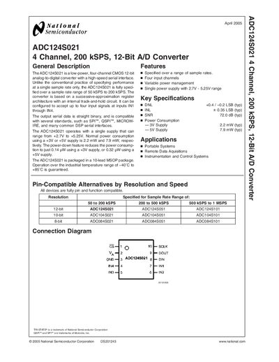
The ADC124S021 is a low‑power, four‑channel CMOS 12‑bit analog‑to‑digital converter with a high‑speed serial interface. It operates from a single supply of +2.7 V to +5.25 V and offers a sample‑rate range of 50 kSPS to 200 kSPS. The device includes variable power‑management features, a built‑in track‑and‑hold circuit, and is packaged in a 10‑lead MSOP.
Key specifications include typical power consumption of 2.2 mW at 3 V and 7.9 mW at 5 V, DNL of +0.4/‑0.2 LSB, SNR of 72 dB, and operation over –40 °C to +85 °C. Ordering information, pin descriptions, absolute maximum ratings, timing diagrams, and application notes are provided for designers.
| Resolution | 12‑bit |
|---|---|
| Sample Rate Range | 50 kSPS – 200 kSPS |
| Supply Voltage | +2.7 V to +5.25 V |
| Power Consumption (3 V) | 2.2 mW typ |
| Power Consumption (5 V) | 7.9 mW typ |
| DNL | +0.4 / -0.2 LSB (typ) |
| SNR | 72 dB (typ) |
| Operating Temperature | -40 °C to +85 °C |
| Package | 10‑lead MSOP |
It operates from a single supply of +2.7 V to +5.25 V.
Typical power consumption is 2.2 mW at a 3 V supply.
The converter can sample up to 200 kSPS, with a specified range of 50 kSPS to 200 kSPS.
It is supplied in a 10‑lead MSOP package.