
The SPD30N06S2-15 is a N-channel enhancement mode power transistor with a maximum continuous current of 30A, a maximum drain-source breakdown voltage of 55V, a maximum on-resistance of 14.7mΩ, and a working temperature range of -55℃ to 175℃. It has anti-avalanche and dv/dt protection functions.
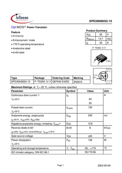
The SPD30N06S2-15 is an N‑channel, enhancement‑mode power transistor designed for high‑current applications up to 30 A continuous and 120 A pulsed. It operates from –55 °C to +175 °C and features an avalanche‑rated energy of 240 mJ.
The document provides detailed electrical characteristics (drain‑source breakdown voltage, gate‑source voltage, on‑state resistance), thermal data (junction‑to‑case resistance 0.69 K/W typical), and typical performance curves such as safe operating area and capacitance values. Contact information for Infineon Technologies AG is included on the final page.
| Continuous drain current (Id) | 30 A |
|---|---|
| Pulsed drain current (Id,pulse) | 120 A |
| Drain‑source breakdown voltage (Vds) | 55 V |
| Gate‑source voltage (Vgs) | +20 V |
| Power dissipation (Pd) | 136 W |
| Operating temperature range | -55 °C to +175 °C |
| Junction‑to‑case thermal resistance (Rθjc) | 0.69 K/W (typ) |
| Input capacitance (Ciss) | 1560 pF (typ) |
| Output capacitance (Coss) | 404 pF (typ) |
| Total gate charge (Qg) | 39‑52 nC (typ) |
The device can carry up to 30 A continuous drain current at 25 °C.
It is rated for a maximum power dissipation of 136 W at 25 °C.
The single‑pulse avalanche energy is rated at 240 mJ.
Typical junction‑to‑case resistance is 0.69 K/W and junction‑to‑ambient is about 100 K/W.