
The MAX4708/MAX4709 are 8-to-1 and dual 4-to-1 fault-protected multiplexers that are pin compatible with the industry-standard DG508/DG509. The MAX4708/MAX4709 are similar to the MAX4508/MAX4509, but these devices do not have clamp diodes to the supply rails on the switch outputs. These multiplexers feature fault-protected inputs, rail-to-rail signal-handling capability, and do not require power-supply sequencing. Both devices offer ±40V overvoltage protection with the supplies off, ±36V protection with the supplies on, and feature 400Ω (max) on-resistance with 15Ω (max) matching between channels. The MAX4708/MAX4709 operate with dual supplies of ±4.5V to ±20V or a single supply of +9V to +36V. All digital inputs have TTL logic-compatible thresholds, ensuring both TTL and CMOS logic compatibility when using a single +12V supply or dual ±15V supplies. For low-voltage applications requiring fault protection, refer to the MAX4711/MAX4712/MAX4713 data sheet. Applications include data-acquisition systems, industrial and process control, avionics, signal routing, redundancy/backup systems, ATE systems, and hot swap systems.
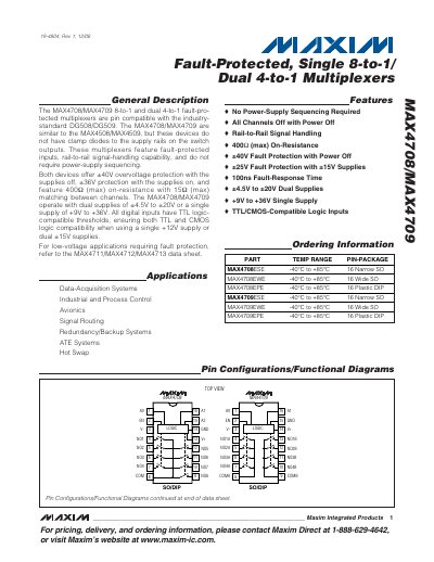
The MAX4708 and MAX4709 are 8‑to‑1 single‑ended or dual 4‑to‑1 fault‑protected analog multiplexers that are pin‑compatible with the DG508/DG509 series. They feature rail‑to‑rail signal handling, no power‑supply sequencing requirement, and TTL/CMOS‑compatible logic inputs.
These devices operate from dual supplies of ±4.5 V to ±20 V or a single supply of +9 V to +36 V, provide ±40 V over‑voltage protection when power is off (±36 V when on), and have a maximum on‑resistance of 400 Ω with 15 Ω channel‑to‑channel matching. Typical fault‑response time is 100 ns.
| Maximum On‑Resistance | 400 Ω (max) |
|---|---|
| Channel‑to‑Channel Matching | 15 Ω (max) |
| Dual‑Supply Voltage Range | ±4.5 V to ±20 V |
| Single‑Supply Voltage Range | +9 V to +36 V |
| Over‑Voltage Protection (Power Off) | ±40 V |
| Over‑Voltage Protection (Power On) | ±36 V |
| Fault‑Response Time | 100 ns |
| Logic Input Thresholds | TTL/CMOS compatible |
The maximum on‑resistance is 400 Ω.
They operate from dual supplies of ±4.5 V to ±20 V or a single supply of +9 V to +36 V.
No, the devices do not require power‑supply sequencing.
The fault‑response time is 100 ns.