
This datasheet provides the functional block diagrams, pin diagrams, electrical characteristics, application examples, etc. of ADM202/ADM203.
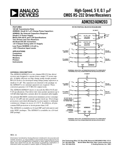
The ADM202/ADM203 is a two‑channel RS‑232 line driver/receiver designed for operation from a single 5 V supply. It uses an on‑chip charge‑pump to generate ±10 V RS‑232 levels, supports up to 120 kB data rates, and includes over‑voltage and ESD protection. The ADM202 version requires external charge‑pump capacitors, while the ADM203 integrates them internally.
The datasheet provides detailed specifications such as output voltage swing (±5 V to ±9 V typical), input logic thresholds (0.8 V low, 2.4 V high), power‑supply current (2.5‑6.0 mA), and pin functions. Mechanical drawings for DIP and SOIC packages are also included.
| Output Voltage Swing | ±5 V to ±9 V (typ) |
|---|---|
| Input Logic Threshold Low | 0.8 V |
| Input Logic Threshold High | 2.4 V |
| Baud Rate | 120 kB |
| Power Supply Current | 2.5‑6.0 mA |
| Supply Voltage | 5 V ±10 % |
| External Capacitors Required (ADM202) | Yes |
| External Capacitors Required (ADM203) | No |
The device supports a maximum data rate of 120 kB.
It operates from a single 5 V supply (±10 %).
No, the ADM203 includes internal charge‑pump capacitors and requires no external capacitors.