
Motorola TMOS Power MOSFET Transistor Device Data is an advanced series of power MOSFETs which utilize Motorola’s High Cell Density TMOS process. These miniature surface mount MOSFETs feature low RDS(on) and true logic level performance. Dual HDTMOS devices are designed for use in low voltage, high speed switching applications where power efficiency is important.
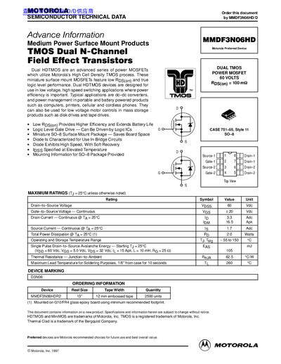
The MMDF3N06HD is a dual N‑channel power MOSFET built with Motorola's High Cell Density TMOS process. It is offered in a miniature SO‑8 surface‑mount package and is intended for low‑voltage, high‑speed switching applications such as DC‑DC converters and portable battery‑powered products.
Key features include a 60 V drain‑to‑source rating, low on‑resistance (≈100 mΩ), logic‑level gate drive, and built‑in diode optimized for fast recovery. The document provides electrical characteristics, safe operating area limits, and recommended soldering procedures for the SO‑8 package.
| Drain‑to‑Source Voltage (Vdss) | 60 V |
|---|---|
| Gate‑to‑Source Voltage (Vgs) | 20 V |
| Continuous Drain Current (Id) | 3.3 A |
| Continuous Source Current (Is) | 1.7 A |
| Total Power Dissipation (Pp) | 2.0 W |
| Operating Temperature Range | -55 °C to 150 °C |
| On‑Resistance (Rds(on)) | ≈100 mΩ |
The device is rated for a maximum drain‑to‑source voltage of 60 V.
Soldering temperature should not exceed 260 °C for more than 10 seconds.
It is supplied in a miniature SO‑8 surface‑mount package.
Typical on‑resistance is about 100 mΩ.