
The MMBFJ175LT1 is a P-channel MOSFET from Motorola. It has a maximum drain-source voltage of 25V and a maximum reverse gate-source voltage of -25V. The maximum power dissipation is 225mW and the maximum junction temperature is 150 degrees Celsius
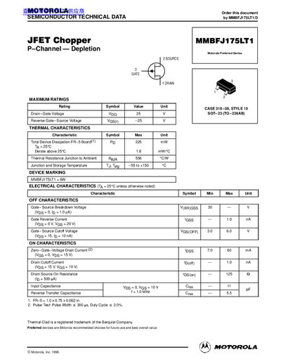
The MMBFJ175LT1 is a P‑channel depletion‑mode JFET offered by Motorola. This datasheet provides maximum voltage and current ratings, thermal limits, and electrical characteristics such as breakdown voltage, leakage currents, and on‑resistance.
Guidelines for surface‑mount implementation are included, covering recommended SOT‑23 footprint dimensions, power‑dissipation calculations, and soldering precautions to avoid thermal stress and ensure reliable assembly.
| Drain‑Gate Voltage (VbDG) | 25 V |
|---|---|
| Reverse Gate‑Source Voltage (Vgs) | -25 V |
| Total Device Dissipation (Pp) | 225 mW |
| Thermal Resistance Junction‑to‑Ambient (RθJA) | 556 °C/W |
| Junction and Storage Temperature Range | -55 °C to +150 °C |
| Gate‑Source Breakdown Voltage (VBRGSS) | 30 V |
| Gate Reverse Current | 1.0 nA |
| Gate‑Source Cutoff Voltage (VGS(off)) | 3.0 V – 6.0 V |
| Zero‑Gate‑Voltage Drain Current (IDss) | 7.0 mA – 60 mA |
| Drain Cutoff Current (ID(off)) | 1.0 nA |
The soldering temperature and time shall not exceed 260 °C for more than 10 seconds.
The delta temperature between the preheat and soldering should be 100 °C or less.
The maximum temperature gradient shall be 5 °C or less.