
This document introduces the characteristics of 54FCT·74FCT273 Octal D Flip-Flop, including ICC, Buffer, Clock, Master Reset, Output, etc.
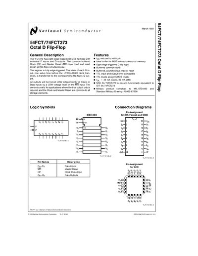
The 54FCT/74FCT273 is an octal D‑type flip‑flop with eight edge‑triggered storage elements, common buffered clock and master‑reset inputs, and TTL‑compatible I/O levels. It is offered in both commercial (74FCT) and military (54FCT) temperature‑range versions.
The document provides detailed absolute maximum ratings, recommended operating conditions, DC and AC electrical characteristics, pin assignments for multiple package types, and physical dimensions. Ordering information and a life‑support policy statement are also included.
| Supply Voltage (Vcc) – 54FCT | 4.5 V to 5.5 V |
|---|---|
| DC Output Current (Iout) | 120 mA |
| Maximum Clock Frequency | 90 MHz |
| Input Capacitance (CIN) | 10 pF |
| Output Capacitance (COUT) | 12 pF |
| Ioc (Leakage Current) | 40 pA |
| Package Types | DIP, Flatpak, SOIC, LCC, Ceramic, Plastic |
The 54FCT version operates from 4.5 V to 5.5 V.
The device can be clocked up to 90 MHz.
Both the 54FCT and 74FCT versions tolerate -0.5 V to +7.0 V with respect to ground.
Yes, the 54FCT is a military‑qualified TTL‑compatible device.