
LM3881 Power Sequencer offers the easiest method to control power up and power down of multiple power supplies (switching or linear regulators).
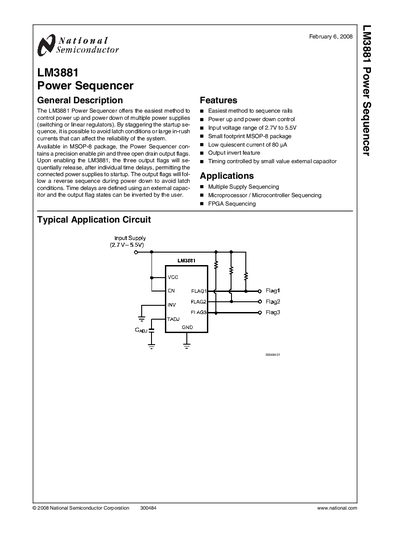
The LM3881 Power Sequencer provides an easy way to control the power‑up and power‑down of multiple regulators by staggering their start‑up sequence. It uses a precision enable pin and three open‑drain output flags (FLAG1‑FLAG3) that release sequentially after programmable delays set by an external timing capacitor on the TADJ pin.
The document includes a general description, pinout, ordering information, absolute maximum and operating ratings, electrical characteristics, block diagram, and application information with typical circuits. It also outlines timing relationships, voltage thresholds, and notes on usage and reliability.
| Input voltage range | 2.7 V to 5.5 V |
|---|---|
| Quiescent current | 80 pA (typical) |
| Number of output flags | 3 open‑drain flags (FLAG1, FLAG2, FLAG3) |
| Maximum VCC to GND rating | -0.3 V to +6.0 V |
| Storage temperature range | -65 °C to +150 °C |
The LM3881 operates with an input supply between 2.7 V and 5.5 V.
It has three open‑drain output flags named FLAG1, FLAG2, and FLAG3.
The typical quiescent current is 80 pA.