
The TLC555 is a monolithic timing circuit fabricated using the TI LinCMOS process. The timer is fully compatible with CMOS, TTL, and MOS logic and operates at frequencies up to 2 MHz. Because of its high input impedance, this device uses smaller timing capacitors than those used by the NE555. As a result, more accurate time delays and oscillations are possible. Power consumption is low across the full range of power supply voltage. Like the NE555, the TLC555 has a trigger level equal to approximately one-third of the supply voltage and a threshold level equal to approximately two-thirds of the supply voltage. These levels can be altered by use of the control voltage terminal (CONT). When the trigger input (TRIG) falls below the trigger level, the flip-flop is set and the output goes high. If TRIG is above the trigger level and the threshold input (THRES) is above the threshold level, the flip-flop is reset and the output goes low.
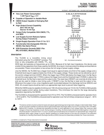
This handbook describes the TLC555 and TLC555Y LinCMOS timers, covering their functional operation, pin assignments, and package options. It includes detailed electrical characteristics such as supply voltage range, output current capability, and timing thresholds.
The document also provides mechanical dimensions, absolute maximum ratings, recommended operating conditions, and handling instructions for ESD‑sensitive devices, along with an important notice about product warranties and critical‑application risks.
| Supply voltage (Vpp) range | 2 V to 15 V |
|---|---|
| Typical sink current | 100 mA |
| Typical source current | 10 mA |
| Operating temperature – TLC555C | 0 °C to 70 °C |
| Operating temperature – TLC5551 | -40 °C to 85 °C |
| Operating temperature – TLC555M | -55 °C to 125 °C |
The TLC555 operates from 2 V up to 15 V supply voltage.
It can sink up to 100 mA (typical) and source up to 10 mA (typical).